What are the important parameters to look for while choosing PCB material ?
[the_ad id=”2778″]In order to design PCBs intelligently it becomes important to understand, among other things, the electrical properties of the board material. Understandably, these materials are the foundations for many circuits, and they are characterized by many different parameters, some related to applications, some to fabrication issues, some to environmental and mechanical concerns. Having a good understanding of different PCB material properties can certainly ease the task of choosing a material for a given set of circuit performance requirements.
It lists numerous material properties, typical values for those properties, conditions under which those values were determined and even applicable measurement methods.
Dielectric Constant, Ɛr
The dielectric constant is a starting point for many PCB material selection processes. Although it can be measured in all three axes of a PCB material the value in the z-direction at a particular test frequency, such as 10 GHz, is typically used for comparison in high-frequency RF/microwave applications. PCB materials with z-axis Dk values ranging from about 2 to 10 are most commonly used for RF/microwave circuit applications.
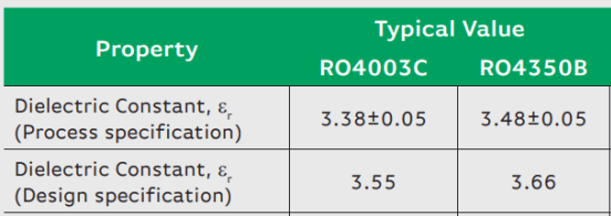
Two different dielectric constant values are given,process and design values. Process dielectric constant value is measured for raw substrate material clamped in a fixture, a test procedure established by IPC. While this is an excellent gauge for PCB material process control and quality assurance, it has several attributes, such as entrapped air, which are not representative of the material’s use in a PCB application. But process dielectric constant value is not suited to be used while doing any kind of simulation modeling or designing any parameter for PCB. For this purpose, design value is better suited as a reference. It is determined by fabricating a micro-strip transmission line of precisely controlled dimensions on a material under test.
Dissipation factor, Df, tanδ
The dissipation factor, Df or tangent delta (tanδ), or loss tangent, is a measure of how much dielectric losses are associated with a particular PCB material.
A PCB material’s Df, for example, can affect the loss of the 50-Ω transmission lines that feed energy to and from an antenna’s radiating elements. To maximize the amount of energy delivered to and from the antenna’s resonant structure, the loss of the feedlines should be minimized, which usually suggests the use of a PCB material with low Df. It is often listed with multiple values for different test frequencies. In general, a PCB material’s dissipation factor will increase with increasing frequency; knowing values at different frequencies provides insight into the broadband loss performance of that material.
Thermal coefficient of Ɛr (TcDk)
Since high-frequency circuits must often perform across a range of operating temperatures, a critical material parameter not always properly considered is thermal coefficient of Ɛr. It is an indicator of how much Ɛr will change as a function of temperature. Sometimes even a small change in the value of a material’s Dk can result in a change in the frequency response of a well-defined resonant circuit, such as a microstrip patch antenna.
Materials with TcDk values of less than 50 ppm/°C are considered well suited to deliver consistent electrical performance with changing operating temperatures. TcDk values can be either positive or negative, with positive values denoting an increase in the Ɛr value for positive changes in temperature, and negative values representing materials having a decrease in Ɛr value with a positive change in temperature.
Electrical strength
Electrical strength is associated with the dielectric strength of a circuit material. The test method measures for the dielectric breakdown point of a material with voltage applied as DC. Although this property may not be critical for lower-power circuits, it can be important for high-power applications or RF/ microwave circuits employing very high DC bias.
Coefficient of Thermal Expansion (CTE)
The coefficient of thermal expansion (CTE), for example, indicates how a circuit material expands and contracts with temperature.It is typically of greatest concern in the z direction or thickness of a circuit material because of the use of plated through holes (PTHs) for electrical connections from one side of a PCB to the other and in multilayer constructions. Excessive z-axis CTE during thermal cycling can damage the PTHs. As a general rule of thumb, a z-axis CTE of less than 70 ppm/°C is considered acceptable. The optimum CTE value is closely matched to the CTE of copper, at 17 ppm/°C.
The CTE of a circuit material in the x and y directions can also be a concern, especially when placing surface-mount devices on the PCB material. If the x-y plane CTE of the material is significantly mismatched from the CTE of a surface-mount device, the expansion and contraction of the circuit material will differ than that of the surface-mount device. With thermal cycling over time, the differences in CTE can cause a work-hardening to occur at the solder joints between the PCB and the surface mount device, potentially harming long-term reliability.
Glass Transition Temperature (Tg)
Glass transition temperature, or Tg, is the temperature range in which a PCB substrate transitions from a glassy, rigid state to a softened, deformable state as polymer chains become more mobile. When the material cools back down, its properties return to their original states. Tg is expressed in units of degrees Celsius (ºC).
Decomposition Temperature (Td)
Decomposition temperature, or Td, is the temperature at which a PCB material chemically decomposes (the material loses at least 5% of mass). Like Tg, Td is expressed in units of degrees Celsius (ºC). A material’s Td is an important ceiling when assembling PCBs, because when a material reaches or surpasses its Td, changes to its properties are not reversible. Contrast this to Tg, glass transition temperature, where properties will return to their original states once the material cools below the Tg range.
Choose a material where you can work in a temperature range that’s higher than Tg but well below Td. Most solder temperatures during PCB assembly are in the 200 ºC to 250 ºC range, so make sure Td is higher than this (luckily, most materials have a Td greater than 320 ºC).
Moisture Absorption
Moisture absorption is the ability of a PCB material to resist water absorption when immersed in water. It is given by percentage increase in weight of a PCB material due to water absorption under controlled conditions as per standard test methods. Most materials have moisture absorption values in the range of 0.01% to 0.20%.
Moisture absorption affects the thermal and electrical properties of the material, as well as the ability of the material to resist conductive anode filament (CAF) formation when a PCB circuit is powered.


