5G Full Duplex Radios- Self Interference Cancellation
“It is generally not possible for radios to receive and transmit on the same frequency band because of the interference that results.” Andrea Goldsmith
The above quote captures a long-held assumption in wireless system design that radios have to operate in half duplex mode i.e., either transmit or receive at time T1 , but can not both simultaneously on the same channel. Today’s mostly practical wireless radios are designed to be half-duplex. For example take a LTE radio if we consider TDD duplex at every 1ms time it can either transmit or receive and in FDD configuration at each 1ms it uses different DL and UL frequecny for transmission and reception. These radio can not support Full Duplex operation because of radio’s Self Interference
Lets consider a practical radio, it has one receive antenna and another transmit chain. Since the receive’s chain input signals are several orders of magnitude lower than the transmit chain’s output signals. suppose if reciever is listening to the same frequency as of transmitter then receiver shall receive the transmitted signal i.e. Tx siganl loop back to the receiver as interference results failure of receiving the desired signal. This loop back interference is also know self interference.

Figure: 1
Recent work has attempted to invalidate Andrea Goldsmith’s assumption. Researchers at Stanford university, Rice and several other groups in industry and academia have proposed various designs to build in-band full-duplex radios.
If it is possible to design a Full duplex radio, it could cut network spectrum needs by half. For example, LTE uses equal width separate uplink and downlink channels (frequencies) to achieve full duplex radio. With Full-duplex radio we could use this a single channel (frequency) to get the same.
Full Duplex Radio Realizations
In theory a Full duplex radio should be simple to accomplish. To achieve Full Duplex Radio, it has to completely cancel the significant self-interference that results from its own transmission to the received signal.We know the signal, we are transmitting and preserves the original baseband signal except for power scaling and frequency shifting to subtract it from the received signal. This subtraction of transmit signal from received can cancle the loop bcak signal i.e. it cancels the self interference. 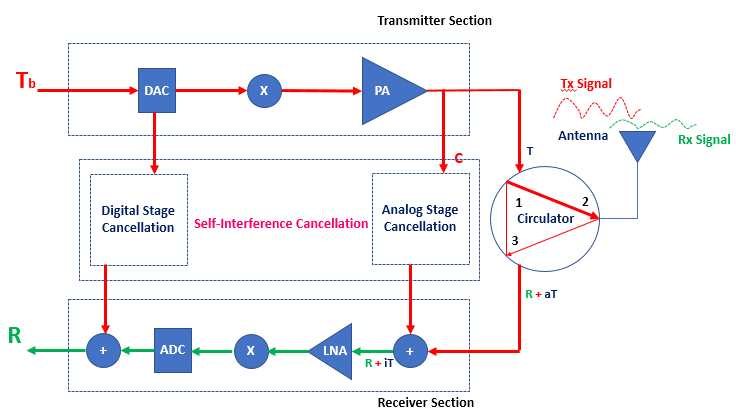
Figure: 2
Components of Self Interference
The main components in self-interference can be classified into three major categories:
- Linear Components
- Non-Linear Components
- Transmitter Noise
Transmitter is consist of linear components like resistor, capacitor etc which result in attenuation and reflection of transmitted signal. Then we have some non-linear components such as transistor with result harmonics of transmitted signal and introduce distortion in input signal. Then another contribution of self interference is the transmitter in-band and side band noise.
Self Interference Cancellation
In practical implementations, exact cancellation of the loop-back interference/self interference may not be feasible because the loop-back interference signal may not be exactly known to either the transmitter or the receiver due involved of different sub-section results in signal distortion, constraints such as dynamic range, resolution of sampling circuitry and phase noise in RF circuitry may restrict the cancellation capability.
A radio has major three sub-sections like Digital sub-section, Analog sub-section and RF sub-section. So this self interference cancellation procedure can be attempt in these sub-section and certain level of self interference cancellation can be achieved.
Different -different technology has different requirements of the self interference cancellation and first technique of it has achieved about 110 dB of cancellation and eliminates self-interference to the noise floor.RF sub-section equipped with component like circulator can eliminate self-interference to about 15 dB.
About 45 dB self interference cancellation can be provided by analog cancellation stage as shown in figure 2. Here we tap the TX chain to obtain a small copy of the transmitted signal just before it goes to the circulator. This copy therefore includes the transmitter noise introduced by the TX chain. The copy of the signal is then passed through a circuit called analog cancellation circuit consists of parallel fixed lines of varying delays and tunable attenuators. The lines are then collected back and added up, and this combined signal is then subtracted from the signal on the receive path. The circuit provides copies of the transmitted signal delayed by different fixed amounts and programmatically attenuated by different variable amounts. The amount of interference cancellation depend how efficiently the cancellation circuit can be tuned and programmed.
Digital Cancellation stage can provides about 50 dB interference cancellation. A signal tapped at the output of DAC is processed at digital cancellation stage and then added up with the received signal in the digital domain.
References:
- http://web.stanford.edu/~skatti/pubs/sigcomm13-fullduplex.pdf
- http://www.ee.iitm.ac.in/~skrishna/papers/spcom2012.pdf
- http://escholarship.org/uc/item/26c9291n#page-1
- http://spectrum.ieee.org/video/telecom/wireless/5g-bytes-full-duplex-explained
- http://ieeexplore.ieee.org/document/7105651/